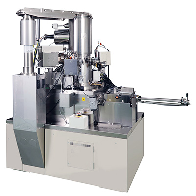
With a minimum spot size of less than 3 nm, the system is capable of line widths less than 8 nm in resist. A 19-bit beam deflection amplifier allows beam steps down to 1.25 Å at 100 kV. Overlay and field stitching accuracy is better than 20 nm in high resolution writing mode. This instrument, in association with etch and deposition capabilities, provides powerful nanofabrication of a wide variety of materials and applications.
Capabilities include:
Due to very high demand, this capability is presently available to current CINT users only. New CINT users can request the electron beam lithography capability by special arrangement with the lead CINT scientist on their proposal. Technical questions may be directed to the specialist listed.
Contact: Anthony James