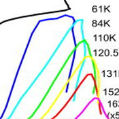
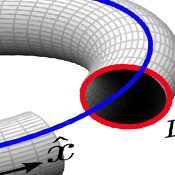
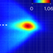
Terahertz (THz) quantum-cascade lasers (QCLs) have witnessed significant progress in recent years in all aspects of their operation, including maximum operating temperature, output power, single-mode operation and beam-shaping, frequency tunability, frequency locking, frequency-comb generation, and demonstration of applications in spectroscopy and imaging.
In this work, a CINT User Team including Sadhvikas Addamane reported terahertz (THz) quantum-cascade lasers (QCLs) based on a three-well GaAs/AlGaAs active region with resonant-phonon depopulation that achieve high operating temperatures at low current densities. CINT highlight slide here.
Full article here: Low Current-Density Thz Quantum-Cascade Lasers with Three-Well Period, Epitaxially Grown with AS2 and AS4 Sources
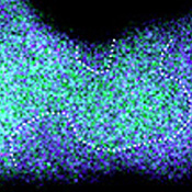
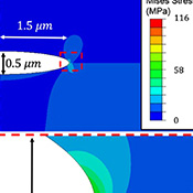
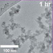
Amorphous grain boundary complexions have been shown to increase the plasticity of nanocrystalline alloys as compared to ordered grain boundaries.
In this work, a CINT User Team including Esther Hessong, Tongjun Niu, Hyosim Kim, Nan Li, Saryu Fensin, and Brad Boyce studied the effect of an important structural descriptor, amorphous complexion thickness, on the plasticity and failure modes of nanocrystalline Cu-Zr through in-situ compression testing, with over 50 micropillars tested. CINT highlight slide here.
Full article here: Thicker Amorphous Grain Boundary Complexions Reduce Plastic Strain Localization in Nanocrystalline Cu-Zr
Material degradation phenomena like corrosion, fatigue cracking, creep, and tribological wear are complex and difficult to predict. By integrating experimental chemical context from X-ray fluorescence (XRF) and mechanical context from nanoindentation alongside atomistic parameters extracted from computational transport simulations (SiMTra), dual deep learning architectures were conducted.
In this study published in Materials Today, a CINT User Team including Brad Boyce explored a novel approach to predicting the life-cycle evolution of a material’s friction coefficient based on the ingestion of multimodal data sources. CINT highlight slide here.
Full article here: Multi-Modal Predictions of Material Degradation: A Case Study on Friction Evolution
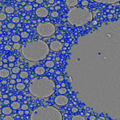
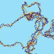
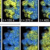
Increasingly large datasets of microscopic images with nanoscale resolution facilitate the development of machine learning methods to identify and analyze subtle physical phenomena embedded within the images.
In this work published in npj computational materials a CINT User Team including Arnab Neogi, Prasad Iyer, Sergei Tretiak, Andrew Jones, Jian-Xin Zhu, Ezra Bussman, Suryakant Mishra, and Tzu-Ming Lu automated the calculation of net magnetic moments and directional orientations of spin-ice configurations microscopic images from honeycomb lattice spin-ice samples. CINT highlight slide here.
Full article here: Deep Generative Learning of Magnetic Frustration in Artificial Spin Ice from Magnetic Force Microscopy Images
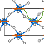
Fractional quantum Hall (FQH) systems are strongly interacting electron systems with topological order. These systems are characterized by novel ground states and fractionally charged and neutral excitations. The neutral excitations are dominated by a low-energy collective magnetoroton mode.
In this study, a CINT User Team including Jian-Xin Zhu derived and used a quasi-one-dimensional model to investigate the ultrafast nonequilibrium dynamics of a laser-driven FQH system within a two-Landau-level approximation. CINT highlight slide here.
Full article here: Laser-Driven Ultrafast Dynamics of a Fractional Quantum Hall System
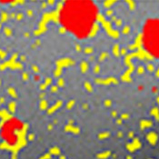
The boundaries between two different crystal phases contain atoms with unique electronic structures and coordination numbers that can significantly influence catalytic performance. Cobalt phosphide adopts Co2P and CoP crystal phases, and both are active for oxygen evolution reaction (OER), which offers the opportunity to improve catalytic activity through the creation of phase boundaries.
In this study, a CINT User Team including Agus Poerwoprajitno showed that mixed-phase Co2P-CoP branched nanoparticles enriched with boundaries between the Co2P and CoP phases can be synthesized by controlled phosphidation of Co branched nanoparticles. CINT highlight slide here.
Full article here: Phase Boundary Engineering of Co2P-CoP Branched Nanoparticles Enhances Cobalt Oxidation for Oxygen Evolution Electrocatalysis
Accurate construction of phase diagrams for aqueous two-phase systems (ATPSs) is essential for identifying two-phase compositions for downstream applications. However, current experimental strategies based on turbidimetric titration are labor-intensive and hindered by inherent inaccuracies.
In this study published in Langmuir, a CINT User Team including Mihee Kim we developed an automated methodology integrating optical microscopy and machine learning to detect microscopic phase separation and define phase boundaries. CINT highlight slide here.
Full article here: Machine Learning-Assisted Phase Diagram Determination in Aqueous Two-Phase Systems
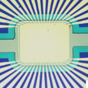
Lorentz reciprocity fundamentally limits the performance of photonic systems by enforcing reciprocal energy exchange between source and detector, which implies a symmetric scattering matrix. In the context of thermal radiation, Lorentz reciprocity manifests as Kirchhoff’s law—the equality of the spectral directional emissivity and absorptivity of a surface. Breaking this reciprocity is important for advancing photonic devices for energy conversion, radiative cooling and mid-infrared sensing and imaging.
In this study published in Nature Communications a CINT User Team including Anatoly Efimov, Chun-Chieh Chang, Hou-Tong Chen, and Abul Azad demonstration of spatiotemporally modulated nonreciprocal metasurfaces operating at mid-infrared frequencies. CINT highlight slide here.
Full article here: Nonreciprocal Scattering and Implications for Thermal Emission Control on a Mid-Infrared Spatiotemporally Modulated Metasurface
Stack pressure and viscoplastic deformation play important roles in improving electrochemical performance and suppressing metal dendrite penetration in solid state batteries. Although progress has been made in understanding these effects, strategies to intentionally leverage viscoplasticity at the cell level remain underdeveloped.
To address this gap, a CINT User Team including John Watt developed viscoplasticity-driven cycling protocols with variable stack pressure conditions. This approach activates rate-dependent stress relaxation during battery operation and can potentially be integrated into existing cycling protocols for sulfide-electrolyte-based solid-state batteries to improve interfacial stability and overall cycling performance. CINT highlight slide here.
Full article here: Stack Pressure Effects and Viscoplastic Deformation in Argyrodite Solid-State Electrolyte
This work presents a machine-learning-based framework for learning reduced-order representations of polymer chain conformations across coarse-grained (CG) and united-atom (UA) fidelities. By employing linear singular value decomposition and nonlinear autoencoders, high-dimensional polymer configurations are compressed into latent spaces with minimal loss of structural accuracy.
In this study, a CINT User Team including Saaketh Desai and Rémi Dingreville demonstrated a near-perfect linear mapping between CG and UA latent spaces, enabling an efficient super-resolution back-mapping procedure that reconstructs high-fidelity UA configurations from CG simulations. CINT highlight slide here.
Full article here: Learning Latent Representations to Bridge Coarse-Grained and Atomistic Resolutions in Polymer Simulations
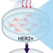
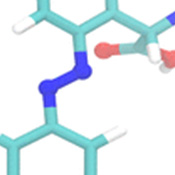
Current HER2-targeted therapies including monoclonal antibodies, antibody-drug conjugates (ADCs) and small-molecule tyrosine kinase inhibitors face limitations such as hepatotoxicity, development of treatment resistance, and subsequent disease relapse.
To overcome these challenges, a CINT User Team including María Nevárez Martínez, Dean Morales, Jim Werner, and Jennifer Hollingsworth combined the specificity of a HER2-targeting affibody molecule (ZHER2:2891-Cys) with the photothermal properties of gold nanorods (AuNRs), forming bioconjugates (Affi–AuNRs) for selective treatment of HER2-positive cancer cells. CINT highlight slide here.
Full article here: Gold Nanorod-Affibody Conjugates Mediate Cancer Photothermal Therapy Under 808 nm LED Irradiation
Soft actuators provide a basis for building robots that can operate in unstructured or extreme environments. Typical pneumatic soft actuators are made from silicone, which lacks biocompatibility and environmental sustainability. Many hydrogel materials have demonstrated compatibility for biomedical and agricultural fields, yet their application in soft robotics remains limited.
In this work, a CINT User Team including Bryan Kaehr sets out to develop a fabrication method to replace synthetic materials with bioderived alternatives and establish the mechanical characterization of their performance. CINT highlight slide here.
Full article here: Engineering Protein-Based Fiber-Reinforced Pneumatic Actuators
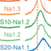
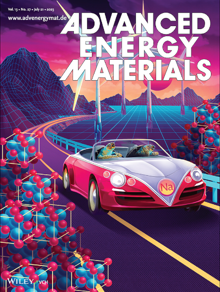
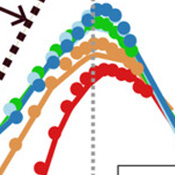
Sodium-ion batteries (SIBs) provide a broader chemical design space for cathodes in terms of composition, crystal structure, and redox chemistry, yet current research largely remains confined to ordered layered frameworks. Recently, Li-excess cation-disordered rock-salt (DRX) cathodes have provided an alternative design space, enabled by their exceptional tunability in composition, stoichiometry, and stability/metastability.
Inspired by these advances, a CINT User Team including John Watt and Madison King significantly expand the compositional space of Na-based cathodes by developing a series of metastable Na-based DRX cathodes based on Na–Ti–Mn–O systems spanning both stoichiometric and over-stoichiometric regimes. CINT highlight slide here.
Full article here: Exploring the Role of Compositional Space of Disordered Rock Salt Na-Ion Battery Cathodes
Understanding mechanisms influencing electrical transport in material systems not only provides a scientific explanation for observed behavior but also offers insight into ways to enhance transport in devices.
In this study, a CINT User Team including Troy Hutchins-Delgado, Adelaide Bradicich, Priyanka Petluru, Michael Lilly, Winson Kuo, Stephen House, and Tzu-Ming Lu report experimental hole mobility of 8 × 10⁴ cm² V⁻¹ s⁻¹ in a Ge0.92Sn0.08, the highest recorded mobility for the GeSn system. CINT highlight slide here.
Full article here: Experimental Characterization and Modeling of High Hole Mobility GeSn Quantum Wells: The Role of Alloy Disorder Scattering
Semiconductor nanomaterials that combine high near-infrared (NIR) photoluminescence efficiency and photostability are limited. Pb-chalcogenide colloidal quantum dots (CQDs), and particularly PbS CQDs, are promising candidates. Nevertheless, the practical implementation of PbS CQDs in optical devices faces intrinsic limitations due to the 8-fold degeneracy of the conduction and valence bands, leading to enhanced nonradiative Auger recombination, hindering applications such as lasing.
In this work, a CINT User Team including Eric Bowes, Victoria Nisoli, Nathan Malone, Jessica Geisenhoff, and Jennifer A. Hollingsworth focuses on the synthesis and optical characterization of core–shell PbS/CdS CQDs emitting at telecommunication wavelengths (1500–1620 nm) with suppressed Auger rates. The team synthesized three series of core/shell PbS/CdS CQDs from different-sized PbS cores via a cation exchange reaction. CINT highlight slide here.
Full article here: Synthesis of Monodisperse PbS/CdS Colloidal Quantum Dots Emitting at Telecommunication Wavelengths with suppressed Auger Rates and Gain Threshold
Recent interest in quantum materials has focused on systems exhibiting both superconductivity and nontrivial band topology as material candidates to realize topological or unconventional superconducting states. So far, superconductivity in most topological materials has been identified as type II.
In this work, a CINT User Team including Jian-Xin Zhu presents magnetotransport studies on the quasi-two-dimensional type I superconductor YbSb2. CINT highlight slide here.
Full article here: Quantum Oscillations and Anisotropic Magnetoresistance in the Quasi-Two-Dimensional Dirac Nodal Line Superconductor YbSb2
The shear response of polyelectrolytes in solutions drives distinct microscopic conformational dynamics whose correlation with macroscopic rheological properties remains an open question.
Using large-scale, fully atomistic molecular dynamics simulations of aqueous solutions of fully sulfonated polystyrene polyelectrolytes, a CINT User Team including Gary Grest probed their conformational dynamics under shear. CINT highlight slide here.
Full article here: Shear Response of Polyelectrolytes in Water
Single-photon emitters are essential components of emerging quantum technologies, including secure communication and quantum computing. Recent advances in deterministic defect engineering — most notably the development of organic color centers (OCCs) — have enabled stable, chemically controllable, and spectrally tunable single-photon emission.
In this review, a CINT User Team including Sergei Tretiak and Han Htoon survey progress in the field from three complementary perspectives: chemical synthesis and quantum defect engineering, computational studies of structure-property relationships and excitonic behavior, and experimental investigations of quantum optical properties. CINT highlight slide here.
Full article here: Quantum Defects in Carbon Nanotubes as Single-Photon Sources
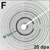
316L stainless steel (316L SS) and high-entropy alloys (HEAs) are leading candidates for radiation-tolerant structural materials in nuclear environments.
In this work, a CINT User Team including Yongqiang Wang conducts a direct quantitative comparison of helium (He) irradiation response, particularly bubble formation, between 316L SS fabricated using laser powder bed fusion (LPBF) and CoCrFeNi HEAs fabricated by laser-directed energy deposition (LDED). CINT highlight slide here.
Full article here: Comparative Study on Helium Ion Irradiation Resistance in Additively Manufactured 316L Stainless Steel and CoCrFeNi High-Entropy Alloy
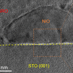
The Hall effect in ferromagnetic (FM) materials is typically linked to magnetization, yet its manifestation in complex heterostructures remains poorly understood.
In this work, a CINT User Team including Pinku Roy, Di Zhang, Nicholas Cucciniello, Sundar Kunwar, and Aiping Chen demonstrates that antiferromagnetic (AFM) NiO can modulate the ferromagnetic state of epitaxial SrRuO3 (SRO). The team systematically investigated the structural, magnetic, and transport properties of SRO/NiO, NiO/SRO, and single-layer SRO films. CINT highlight slide here.
Full article here: Coupling of Anomalous Hall and Planar Hall Effects in Ferromagnet/Antiferromagnet Bilayers
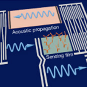
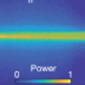
Surface acoustic waves (SAWs) enable a wide array of technologies, including radiofrequency filters, chemical and biological sensors, acousto-optic devices, acoustic control of microfluidic flow in lab-on-a-chip systems and quantum phononics. Although numerous methods exist for generating SAWs, they each have intrinsic limitations that inhibit performance, operation at high frequencies and use in systems constrained in size, weight and power.
In this work, a CINT User Team including Matt Eichenfield presented a completely solid-state, single-chip SAW phonon laser consisting of a lithium niobate SAW resonator with an internal, d.c. electrically injected and broadband semiconductor gain medium with <0.15 mm2 footprint. CINT highlight slide here.
Full article here: An Electrically Injected Solid-State Surface Acoustic Wave Phonon Laser

For semicrystalline polyolefin thermoplastics, the balance between interconnected ordered crystalline and disordered amorphous regions is paramount to their performance and processability. However, contemporary manufacturing strategies, from injection molding to three-dimensional (3D) printing, result in monolithic objects, unable to spatially encode crystallinity.
In this study published in published in Science, a CINT User Team including Bryan Kaehr developed a light-based approach for mechanically fabricating robust polyolefin thermoplastics with microscopic control over crystallinity in 3D space. CINT highlight slide here.
Full article here: Lithographic Crystallinity Regulation in Additive Fabrication of Thermoplastics (CRAFT)
The propagation path of topologically protected states is bound to the interface between regions with different topology, and as such, the functionality of linear photonic devices leveraging these states is fixed during fabrication. Instead, to realize reconfigurable topology, one both needs a method for dynamically altering a system’s topology, e.g., through the addition of energy somewhere that yields a nonlinear change in the system’s Hamiltonian, and as a method for reverting that change to return the system to its original state, demanding some form of dissipation. However, traditional topological classification methods cannot be applied to localized nonlinearities, as they inherently prohibit a band structure-based description by breaking translational symmetry.
In this study published in Light: Science and Applications, a CINT User Team including Alexander Cerjan proposed a mechanism for dynamic control over a driven dissipative system’s local topology, yielding reconfigurable topological interfaces and thus tunable paths for protected routing. CINT highlight slide here.
Full article here: Dynamically Reconfigurable Topological Routing in Nonlinear Photonic Systems
Free-space optical metasurfaces are typically engineered only in their in-plane dimension and are therefore comprised of nanostructures that are all the same height. A growing body of theory work has suggested that metasurfaces become more capable if they are also engineered in their out-of-plane dimension. However, experimental realization of such metasurfaces is rare as standard nanofabrication processes do not readily support elaborate height profiles at the nanoscale in high-index materials.
In this paper, a CINT User Team including Stephanie Malek and Chloe Dorion presented several experimental demonstrations of multi-height metasurfaces made of gallium nitride that support high quality factor optical resonances in the visible and near infrared. To do so, the team developed not only a flexible nanofabrication method but also a new design framework that reconsiders common assumptions in metasurface design. CINT highlight slide here.
Full article here: Nonlocal Metasurfaces with Lithographically Defined Vertical Symmetry Breaking
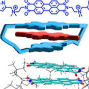
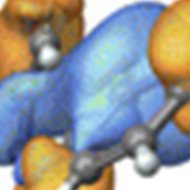
Organic molecules that absorb light can be connected together like building blocks to create materials for solar cells and electronics. How these molecules are attached, whether loosely stacked or chemically linked, dramatically changes how energy and electrical charges move through the material.
In this study, a CINT User Team including Sergei Tretiak employed first-principle calculations to elucidate structure–property relationships in three perylenediimide (PDI) trimer systems: a noncovalent assembly (u-PDI3), a stapled assembly (t-PDI3), and a folded (foldamer) assembly (s-PDI3) in aqueous solvent. These results showed how tethering controls the interchromophore geometry, particularly twist angles and slip displacements, which determine electronic coupling patterns. CINT highlight slide here.
Full article here: Covalent Control of Excitonic Interactions in Perylenediimide Trimers: A Computational Study

Transition metal (i.e., Mn, Fe, Cr) and chalcogen (Se) substituents are introduced into single-crystalline NiPS3, and the evolution of the two emergent quasi-particle excitations characteristic to the XXZ correlated antiferromagnetism of NiPS3 (i.e., spin orbit entangled exciton (SOX) and two-magnon scattering (2M )) are investigated as functions of substituent concentration through comprehensive room- and low-temperature photoluminescence (PL) and Raman spectroscopy studies. These findings are further correlated with the magnetic properties of the same set of compounds reported in prior studies.
In this work, a CINT User Team including Cong Tai Trinh, Na Liu, Rijan Karkee, Vigneshwaran Chandrasekaran, Andrew Jones, Michael Pettes, and Han Htoon revealed that the SOX emission intensities and linewidths are mainly controlled by the magnetic anisotropy and spin orientations, and are strongly suppressed by the introduction of substituents. CINT highlight slide here.
Full article here: Manipulation of Emergent Collective Excitations via Composition Control in Mixed MPX3 Correlated 2D Antiferromagnets
Metal oxides have strong potential for long-duration thermochemical energy storage, but most studies have focused on bulk and microscale measurements. Designing nanostructured thermochemical materials may enable better reaction reversibility and faster kinetics, making it important to understand their behavior at the nanoscale.
In this work published in Nano Letters, a CINT User Team including Stephen House used advanced environmental transmission electron microscopy, combined with time-resolved imaging with electron energy loss spectroscopy, to examine cobalt oxide nanoparticles with high spatial and temporal resolution during thermochemical cycling under realistic operating conditions. CINT highlight slide here.
Full article here: Revealing Progressive Degradation of Cobalt Oxide Nanoparticles During Thermochemical Redox Cycling via Operando STEM-EELS

The topological properties of a material depend on its symmetries, parameters, and spatial dimension. Changes in these properties due to parameter and symmetry variations can be understood by computing the corresponding topological invariant. Since topological invariants are typically defined for a fixed spatial dimension, there is no existing framework to understand the effects of changing spatial dimensions via invariants.
In this work recently published in Communications Physics, a CINT User Team including Alexander Cerjan introduced a framework to study topological phase transitions as a system’s dimensionality is altered using real-space topological markers. CINT highlight slide here.
Full article here: Dimensional Crossover of Class D Real-Space Topological Invariants
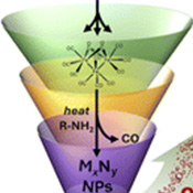
Low-temperature, scalable routes to transition metal nitride (TMN) nanoparticles are desirable for a wide range of applications, yet their synthesis typically requires high temperatures (>350 °C) and reactive gas environments (e.g., NH3 or H2/N2)
In this work, a CINT User Team including Sergei Ivanov and John Watt report a colloidal synthesis of mono- and bimetallic TMN nanoparticles using preformed metal carbonyl clusters as precursors and urea or diethylenetriamine (DETA) as nitrogen sources. This strategy enables access to size-controlled, phase-pure ε-Fe3Nx and FeyNi3−yN nanoparticles at temperatures below 300 °C, without the need for flowing reactive gas atmospheres. CINT highlight slide here.
Full article here: Low-Temperature Access to Active Iron and Iron/Nickel Nitrides as Potential Electrocatalysts for the Oxygen Evolution Reaction
Resistive switching (RS) devices with ultra-low-voltage threshold and reliable switching repeatability exhibits great potential applications in energy-efficient data storage and neuromorphic computing. Understanding switching mechanisms at nanoscale is critical to design RS devices with improved performance.
In this work published in Advanced Functional Materials, a CINT User Team including Di Zhang, Sundar Kunwar, Michael Pettes, John Watt, Winson Kuo, and Aiping Chen fabricated a lamella memristive device using the focused ion beam (FIB) method based on a metal/TiOx/TiN/Si structure. CINT highlight slide here.
Full article here: In Situ Study of Resistive Switching in a Nitride-Based Memristive Devic
Sodium solid-state batteries (Na-SSBs) are an emerging alternative to lithium-ion batteries that have dominated the energy storage market for the last three decades. Compared to lithium, sodium is abundant and evenly distributed in the Earth's crust, making it an attractive candidate for energy storage solutions, such as sodium-ion and sodium-metal batteries. However, unlike lithium, sodium cannot intercalate effectively into graphite, necessitating the development of alternative anodes.
In this study published in Advanced Materials, a CINT User Team including John Watt presented the first reported use of reactive carbide precursors, ZrC and SiC, for the solid-state synthesis of NZSP. This novel approach leverages an exothermic reaction pathway that facilitates improved densification, phase purity, and microstructural distribution. CINT highlight slide here.
Full article here: Reactive Carbide-Based Synthesis and Microstructure of NASICON Sodium Metal All Solid-State Electrolyte
Resolving molecular chirality on the atomic scale remains a critical challenge in chemistry. Conventional Optical Circular Dichroism spectroscopy often overlooks subtle and localized structural features.
In this study a CINT User Team computationally investigated site-specific X-ray circular dichroism (XCD) across a series of trans-azobenzene derivatives to deconstruct and interpret chiroptical signals at the atomic level. This modeling reveals that XCD is capable of distinguishing dichroic contributions arising from both a local chiral center and a global molecular twist, revealing their intricate interplay and potential for constructive or destructive interference. CINT highlight slide here.
Full article here: Deconstructing Chirality: Probing Local and Nonlocal Effects in Azobenzene Derivatives with X-ray Circular Dichroism

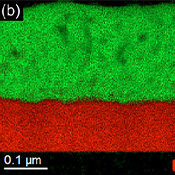
Solid-state lithium batteries promise higher energy density and improved safety compared with conventional liquid-electrolyte batteries, but their performance is often limited by lithium dendrite growth — tiny metallic filaments that penetrate and short-circuit the electrolyte.
In this study a CINT User Team introduced a new grain boundary–engineered garnet electrolyte, where zirconia (ZrO₂) nanoparticles form in situ during sintering at the interfaces between grains of the standard Li₆.₄La₃Zr₁.₄Ta₀.₆O₁₂ (LLZTO) material. The process uses a reactive tantalum carbide (TaC) additive that decomposes to release oxygen and substitute tantalum for zirconium in the crystal lattice, creating a two-phase oxide–oxide composite with controlled microstructure and chemistry. CINT highlight slide here.
Full article here: Grain Boundary Zirconia-Modified Garnet Solid-State Electrolyte
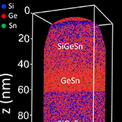
GeSn is an emerging material with potential applications in nex-generation integrated optoelectronics and quantum information processing. While GeSn/SiGeSn quantum wells exhibit promising optical properties, their electrical transport characteristics and governing electrostatics in gated structures remain unexplored.
In this work, a CINT User Team fabricated heterostructure field-effect transistors with two different well/barrier compositions. Remarkably, devices with SiGeSn barriers exhibited mobilities several times higher than previously reported GeSn quantum wells with conventional germanium barriers at low carrier densities. These results contradict the initial expectation that the ternary alloy would introduce more scattering. Using atom probe tomography at Dartmouth, the team identified short-range ordering of silicon atoms in the SiGeSn barrier layers, which may template improved ordering in the GeSn quantum well during growth and reduce alloy scattering effects. CINT highlight slide here.
Full article here: High Mobility and Electrostatics in GeSn Quantum Wells With SiGeSn Barriers
Ion exchange membranes have been the focus of continued research for applications such as electrolysis, electrodialysis, energy conversion, and energy storage. Ion exchange membranes are broadly classified by the charge of the mobile counterion, being either a cation exchange membrane (or, when specifically referring to protons, a proton exchange membrane, or PEM) or an anion exchange membrane (AEM). Particularly for applications in fuel cells, AEMs are a research focus because they avoid the need for expensive catalysts such as platinum typically used in PEM-based fuel cells. A multitude of synthetic routes for AEMs are found in the literature, resulting in polymers with various cationic functional groups.
In this work, a CINT User Team including Amalie Frischknecht investigated the morphology and transport properties of a new class of polymers using atomistic molecular dynamics simulations, which are functionalized with quaternary ammonium groups for use as anion exchange membranes. CINT highlight slide here.
Full article here: Investigating Morphology and Diffusion in Simulations of Precise Anion-Conducting Polymers

Flat bands in twisted materials have attracted considerable attention due to the emergence of correlated phases that can be associated with the non-Wannier-representable nature of its single-particle states. Specifically, these bands can exhibit a class of topology that can be nullified by the addition of trivial bands, termed fragile topology, which has required an expansion of prior classification schemes. However, existing approaches for predicting fragile topology rely on momentum-space methods, e.g., Wilson loops, presenting a fundamental challenge for using fragile topology as a predictor of correlated phases in aperiodic systems, such as incommensurate twist angles in moiré materials.
In this work, a CINT-led User Team including Ki Young Lee, Stephan Yong, and Alexander Cerjan developed a ℤ2 energy-resolved topological marker for classifying fragile phases using a system’s position-space description, enabling the direct classification of finite, disordered, and aperiodic materials. CINT highlight slide here.
Full article here: Classification of Fragile Topology Enabled by Matrix Homotopy
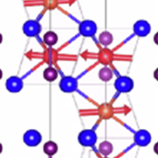
Magnetic van der Waals (vdW) materials exhibit a profound interconnectedness between their various degrees of freedom, pointing to a wealth of potential applications in low-power and high-speed spintronic devices. Recently, light-matter interactions have been leveraged as robust, dynamic pathways to gain control over the properties of vdW magnets through the use of ultrafast pulses of light.
In this work recently published in npj Spintronics, a CINT User Team including Luis Martinez, Prashant Padmanabhan, and Michael Pettes utilized ultrafast photoexcitation to drive coherent lattice oscillations in the layered ferrimagnetic crystal Mn3Si2Te6, which significantly stiffen below the magnetic ordering temperature. The team suggested that this is due to an exchange-mediated contraction of the lattice, stemming from strong magneto-structural coupling in this material. CINT highlight slide here.
Full article here: Dynamic Signatures of Spin-Lattice Coupling in the Layered Ferrimagnet Mn3Si2Te6

In addition to a plethora of emergent phenomena, the spatial topology of optical vortices enables an array of applications in optical communications and quantum information science. Multibeam nonlinear optical processes, augmented by optical vortices, are essential in this context, providing robust access to an infinitely large set of quantum states associated with the orbital angular momentum of light.
In this work recently published and featured on the cover of ACS Nano, a CINT User Team including Prashant Padmanabhan, Tenzin Norden, Luis Martinez, Nehan Tarefder, Luke McClintock, Jinkyoung Yoo, Jian-Xin Zhu, Antoinette Taylor, Rohit Prasankumar, and Wilton Kort-Kamp pushed the boundaries of vortex nonlinear optics to the ultimate limits of material dimensionality. By exploiting multipulse difference frequency, sum frequency, and four-wave mixing in monolayer quantum materials, the team demonstrates their ability to independently control the orbital angular momentum and radial distribution of vortex light-fields in addition to their wavelength. CINT highlight slide here.
Full article here: Twisted Nonlinear Optics in Monolayer van der Waals Crystals
The additional layer degree of freedom in trilayer moiré superlattices of transition metal dichalcogenides enables the emergence of novel excitonic species, such as quadrupolar excitons, which exhibit unique excitonic interactions and hold promise for realizing intriguing excitonic phases and their quantum phase transitions. Concurrently, the presence of strong electronic correlations in moiré superlattices, as exemplified by the observations of Mott insulators and generalized Wigner crystals, offers a direct route to manipulate these new excitonic states and the resulting collective excitonic phases.
In this recent Nature Photonics article, a CINT User Team including Shi-Zeng Lin demonstrates that strong exciton–exciton and electron–exciton interactions, both stemming from robust electron correlations, can be harnessed to controllably drive transitions between quadrupolar and dipolar excitons. CINT highlight slide here.
Full article here: Strong-Interaction-Driven Quadrupolar-to-Dipolar Exciton Transitions in a Trilayer Moiré Superlattice

The original proposal of quantum key distribution (QKD) was based on ideal single-photon sources, which, 40 years later, are still challenging to develop. Therefore, the development of decoy-state protocols using weak coherent states (WCS) from lasers set the frontier in terms of secure-key rates and distances.
In this article published in PRX Quantum, a CINT User Team including Eric Bowes and Jennifer Hollingsworth proposed and experimentally demonstrated two simple-to-implement QKD protocols that allow practical far from ideal sub-Poissonian photon sources to outperform state-of-the-art WCS. CINT highlight slide here.
Full article here: Decoy-State and Purification Protocols for Superior Quantum Key Distribution with Imperfect Quantum-Dot-Based Single-Photon Sources: Theory and Experiment
Enzymes are nature’s catalysts, but their instability outside native environments limits practical applications. Metal–organic frameworks (MOFs) offer a promising platform for enzyme immobilization, enhancing stability, and reusability through their tunable porosity and crystallinity.
In this Chemistry of Materials article, a CINT User Team including John Watt reports that NH4OH modulates crystal morphology, enzyme activity, and nucleation behavior, with higher concentrations leading to partial enzyme denaturation and reduced catalytic performance. By integrating time-resolved cryo-TEM with activity assays, we uncover how modulator concentration impacts early stage crystallization and enzyme folding, a mechanistic insight not previously demonstrated in MOF systems. CINT highlight slide here.
Full article here: Role of Ammonium Hydroxide on Glucose Oxidase Immobilized in Metal–Azolate Framework-7 Enzyme Activity
The microscopic understanding of probing and controlling molecular chirality is of considerable interest. Numerous spectroscopic techniques are capable of monitoring molecular asymmetry and its consequences, ranging from the infrared to the X-ray regime. Resonant X-rays have long been used to investigate local atomic sites within molecules thanks to the localized nature of core electronic transitions. These techniques can be used to determine the extent to which chirality is a local versus a delocalized property. However, how to systematically partition dichroic contributions from the point of view of electronic structure simulations remains an open question.
In this work, a CINT User Team introduced the concept of chiral population analysis that connects chirality to the atomic orbital picture. In analogy with Mulliken population analysis, which assigns charges to atomic orbitals, chiral populations allow the dichroic response to be distributed among the participating atomic orbitals. CINT highlight slide here.
Full article here: Chiral Population Analysis: A Real Space Visualization of X-Ray Circular Dichroism
Silicon-based photonic integrated circuits (Si-PICs) have evolved over the past four decades, revolutionizing optical communication, sensing, artificial intelligence training, and quantum technologies. The successful integration of on-chip laser sources marked a major breakthrough in silicon photonics, yet further advancements are essential to unlock its full potential and expand its applications.
In this Optica article, a CINT User Team including Weng Chow reports high-Q locking configurations, an approach that leverages a broadband external cavity, effectively mitigating thermorefractive noise and mode-hopping while ensuring stable operation. CINT highlight slide here.
Full article here: Sub-Hertz-Linewidth Hybrid-Integrated Laser for Isolator-Free Silicon Photonics
Landau levels have been central to the discovery of exotic quantum phases and their unprecedentedly deep roots in geometry and topology. A powerful concept called “vortexability” extends this framework to moiré systems.
In this Physical Review Letter, a CINT User Team including Shi-Zeng Lin shows that vortexable systems support not only Landau-level-like flat bands but also entirely new types with distinct topological properties. CINT highlight slide here.
Full article here: Symmetry-Based Classification of Exact Flat Bands in SIngle and Bilayer Moiré Systems

Excitonic insulators formed by the pairing of electrons and holes due to Coulomb interactions were first predicted more than 50 years ago. Since then, excitonic insulators have been observed in various classes of materials, including quantum Hall bilayers, graphite, transition metal chalcogenides, and more recently in moiré superlattices.
In this Physical Review Letters article, a CINT User Team with Michael Pettes reports the experimental observation of a spin-triplet excitonic insulator in the ultra-quantum limit of a three-dimensional topological material HfTe5, observing that the spin-polarized zeroth Landau bands dispersing along the field direction cross each other beyond a characteristic magnetic field in HfTe5, forming the one-dimensional Weyl mode. CINT highlight slide here.
Full article here: Possible Spin-Triplet Excitonic Insulator in the Ultraquantum Limit of HfTe 5

Strain engineering is vital for tuning the optical and spin properties of solid-state color centers, enhancing spin coherence and compensating emission wavelength shift.
In this article published in Nature Communications, a CINT User Team including Matt Eichenfield developed an all-optical approach to directly modify the local strain of color centers at the nanoscale by migrating the nearby defect CINT highlight slide here.
Full article here: All-Optical Reconfiguration of Single Silicon-Vacancy Centers in Diamond for Non-Volatile Memories
Quantum ghost imaging is a method that utilizes the correlated detection of two photons to generate an image. One photon is detected by an imaging sensor and the other by a single-element bucket detector. The selection of the imaging sensor and its capabilities relative to the bucket detector impact the quality of the ghost images.
In this work, a CINT User Team including Duncan Ryan examined a SPAD array and a photocathode detector as imaging sensors for quantum ghost imaging. The team discusses how to achieve optimal images using these two technologies and demonstrated that these devices are able to generate ghost images at 1Hz frame rates, expanding the technique to biologically relevant time scales. CINT highlight slide here.
Full article here: Time-Resolved Detectors for Quantum Ghost Imaging
Using all-atom molecular dynamics simulations and a variety of experimental methods, it was previously reported on a linear polyethylene with pendant phenyl sulfonated groups precisely on every fifth carbon along the backbone. With increasing relative humidity this fluorine-free polymer self-assembled to form nanoscale water channels and exhibited exceptional proton conductivity.
In this work, a CINT User Team including Amalie Frischknecht quantitatively describe the nature of the water channels using the characteristic distance, channel width distribution, the area per sulfonate group at the hydrophilic / hydrophobic interface, and the fractal dimension. Notably, the channel widths and the areas per sulfonate group are nominally independent of the level of sulfonation, while depending significantly on the level of hydration. The fractal dimension of the water channels correlates strongly with the water diffusion coefficients calculated from the MD simulations. These findings demonstrate that the 5PhSH-Y hydrocarbon copolymers can be modified to tune properties particularly proton conductivity. CINT highlight slide here.
Full article here: Effect of Sulfonation Level on the Percolated Morphology and Proton Conductivity of Hydrated Fluorine-Free Copolymers: Experiments and Simulations
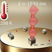
Single photons are cornerstones of quantum technologies. The need for an ultrafast, bright, and stable photon source emitting in the telecom-band at ∼1550 nm, ideally operating at room temperature, has resulted in a decades-long quest.
In this ACS Nano research, stable colloidal PbS/CdS quantum dots are embedded in a solution-synthesized nanoparticle-on-mirror cavity. Single cavity-coupled quantum dots experience extreme Purcell factors up to 10,700, resulting in ultrafast emission lifetimes of 65 ps, along with near-complete blinking suppression. As a result, 12 million single photons are emitted per second affording a single photon source at 1550 nm that is more than two orders of magnitude brighter than previously possible at room-temperature. CINT highlight slide here.
Full article here: Solution-Processed Ultrafast, Room-Temperature Single-Photon Source at 1550 nm
Material design and accessible manufacturing are often at odds with each other, calling for creative solutions to adapt high-performance materials to available processes.
In this research recently published in Nature Communications, a CINT User Team provides a solution to make thermoset materials amenable to vacuum forming. Specifically, an ambient polymerization is used to transition a liquid monomeric solution to an elastomeric gel. CINT highlight slide here.
Full article here: Frontal Polymerization of Thermosets to Enable Vacuum-Formed Structural Electronics
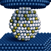
The adhesion of nanoparticles to their supports is key to their performance and stability. However, scientific advances in this area have been hampered by the difficulty of experimentally probing adhesion. To date, only a single technique has been developed that can directly measure nanoparticle adhesion, and this technique is inherently limited to monometallic systems.
In this , a CINT User Team presents a versatile technique for the direct measurement of adhesion for bimetallic nanoparticle systems. CINT highlight slide here.
Full article here: In Situ Measurement of Adhesion for Multimetallic Nanoparticles
Realizing innovative composite materials with passive thermal management capabilities and minimal ecological footprints is a challenging but much sought-after goal that would have a transformative effect on renewable energy sciences.
In this , a CINT User Team demonstrates an environmentally friendly metasurface utilizing vanadium dioxide (VO 2) that offers responsiveness to ambient temperature and potentially long-term stability. CINT highlight slide here.
Full article here: Passive Radiative Thermal Management Using Phase-Change Metasurfaces
All-solid-state lithium–metal batteries hold great promise because of their high energy density stemming from using an energy-dense lithium–metal anode. However, mitigating the dendritic lithium–metal growth, originating from heterogeneous lithium–metal deposition, is a priority to suppress short-circuit and extend cycle life.
In this research recently published in ACS Nano, a CINT User Team employs direct current (DC) magnetron sputter coating to deposit tin (Sn) and carbon (C) on a stainless steel (SUS) current collector to achieve uniform lithium–metal plating and improve cycling performance. CINT highlight slide here.
Full article here: Tin–Carbon Dual Buffer Layer to Suppress Lithium Dendrite Growth in All-Solid-State Batteries.
Developing high-performance plasma-facing materials (PFMs) is one of the most urgent and challenging tasks in the field of material for the realization of commercial fusion reactors because PFM suffers from harsh environments, including irradiation by high fluxes of hydrogen isotopes (D and T) and He plasma.
In this Acta Materialia article, a CINT User Team studies the radiation resistance of tungsten-containing amorphous refractory multi-component alloy film via He plasma irradiation. CINT highlight slide here.
Full article here: A New Type of Plasma Irradiation-Resistant Amorphous TiZrHfTaW refractory Multi-Component Alloy
Quantum spin liquids (QSLs) are exotic phases of matter that avoid long-range ordering at zero temperature . Rather, these phases are characterized by topological order associated with fractionalization, emergent gauge fields, and Abelian or non-Abelian anyonic quasiparticles. Interest in QSLs was initially driven by proposals linking them to high-temperature superconductivity upon doping . Further understanding of QSLs showed that they have promising applications in topological quantum computation . Despite such great interest and potential applications, a definitive experimental observation of these phases is still lacking after decades of search.
In this Physical Review Letters article, a CINT User Team including CINT Scientist Shi-Zeng Lin studies quasiparticle interference (QPI) in the Kitaev quantum spin liquid (QSL) for electrons tunneling into the QSL. Local tunneling conductance around a spin vacancy or localized vison reveals unique features associated with fractionalized Majorana fermions, chargons, and visons. In certain parameter regimes, the single-spinon density of states and momentum dispersion can both be directly extracted from the tunneling conductance. Their results suggest that QPI is a promising tool for identifying the Kitaev QSL and its fractionalized excitations. CINT highlight slide here.
Full article here: Quasiparticle Interference in Kitaev Quantum Spin Liquids

The diode effect has been advanced by the introduction of topology into condensed matter physics, which imposes great potential for future optoelectronic devices. Such applications have been demonstrated in two-dimensional thin films or heterostructures but not yet in prototype three-dimensional topological insulators.
In this PNAS article, a CINT User Team demonstrates a topological diode effect on the surface of a three-dimensional material, SmB
Full article here: Realizing a Topological diode Effect on the Surface of a Topological Kondo Insulator
Quantifying the material properties of hard biological materials can improve understanding of the relationships between form, function, and performance. This study illustrates the use of nanoindentation as a tool for evaluating material properties in a comparative biology framework.
In this Integrative Organismal Biology article, a CINT User Team provides a step-by-step guide for comparative and evolutionary biologists illustrating the collection and analysis of nanoindentation data from samples of artiodactyl skull bones. CINT highlight slide here.
Full article here: A Brief Introductory Guide to Nanoindentation for Comparative and Evolutionary Biologists, with a Case Study of Bone Material Property Diversity across Artiodactyl Skulls
With the advent of additive manufacturing, manipulation of typical microstructural elements such as grain size, texture, and defect densities is now possible at a faster time scale. While the processing–structure–property relationship in additive manufactured metals has been well studied over the past decade, little work has been done in understanding how this process affects the dynamic behavior of materials.
In this Journal of Applied Physics article, a CINT User Team postulates that additive manufacturing can be used to alter materials' microstructure and used to enhance its dynamic strength. CINT highlight slide here.
Full article here: Tailoring Additive Manufacturing to Optimize Dynamic Properties in 316l Stainless Steel
Since the 1970s, materials selection for application in future thermonuclear fusion reactors has posed a significant challenge for materials science and metallurgy. The deuterium-tritium fusion reaction exposes fusion reactors and their structural materials to exceptionally harsh environmental conditions.
In this Advanced Science article, a CINT User Team demonstrates that reducing alloying elements in RHEAs is feasible without compromising radiation tolerance. Herein, two Highly Concentrated Refractory Alloys (HCRAs) — W 53Ta 44V 3 and W 53Ta 42V 5 (at.%) — were synthesized and investigated. CINT highlight slide here.
Full article here: High Radiation Resistance in the Binary W-Ta System Through Small V Additions: A New Paradigm for Nuclear Fusion Materials
Catalysts based on Pt nanoparticles supported on carbon (Pt/C) are widely used in proton-exchange membrane fuel cell (PEMFC) cathodes. The Pt weight percent (wt%) and the type of carbon used influence the PEMFC performance and durability, but the mechanism of this influence remains poorly understood
In this Electrochimica Acta article, a CINT User Team systematically investigate the effect of catalyst metal content and the type of carbon support on PEMFC performance and durability by employing two types of commercially available Pt/C catalysts. CINT highlight slide here.
Full article here: Effect of the Catalyst Metal Content and the Carbon Support on Proton-Exchange Membrane Fuel Cells Performance and Durability

Low-current multilevel programmability with inherent non-volatility and high stability of resistance states is required for both multi-bit memory storage and deep learning accelerators but is difficult to achieve.
In this Advanced Functional Materials article, a CINT User Team realizes >512 (>9 bits) distinct non-volatile conductance levels with stable retention for each state with current levels down to the nanoampere range, highly promising for potential integration with small processing nodes with ultra-low power consumption requirements. CINT highlight slide here.
Full article here: Ultra-Fast Non-Volatile Resistive Switching Devices with Over 512 Distinct and Stable Levels for Memory and Neuromorphic Computing
Alkaline water electrolysis holds promise in decarbonizing the global economy by enabling renewable hydrogen production with non-precious group metal catalysts. Anion exchange membranes are an important component of alkaline water electrolyzers and would ideally be durable while allowing for high hydroxide conductivity.
In this Journal of Membrane Science article, a CINT User Team performs atomistic molecular dynamics (MD) simulations of several PAP polymers at experimentally relevant hydration levels and polymer ion exchange capacities (IECs) to gain nanoscale insight into their properties and to help elucidate the trade-offs that result from tuning the IECs through the polymer stoichiometry.. CINT highlight slide here.
Full article here: Effect of Stoichiometry and Hydration Level on Water Domain Size and Transport in Poly(aryl piperidinium) Alkaline Anion-exchange Membranes
GeSn is a group-IV alloy with immense potential to advance microelectronics technology due to its intrinsic compatibility with existing Si CMOS processes.
In this ACS Applied Materials & Interfaces article, a CINT User Team presents a polycrystalline thin-film GeSn phototransistor on a fused silica substrate with a Sn composition of ∼10%, showing a photoresponse in the short-wave infrared wavelength range, critical for emerging sensing applications. CINT highlight slide here.
Full article here: Gate-Tunable Short-Wave Infrared Polycrystalline GeSn Phototransistors on Noncrystalline Substrates
The coexistence of electric and magnetic order in multiferroics has made these materials the subject of intense investigation, due to the possibility of indirectly manipulating charge, spin, and orbital degrees of freedom by exploiting the strong coupling between these various quantities.
In this Nanophotonics article, a CINT User Team presents an optical pump-terahertz (THz) probe study on multiferroic Eu 0.75Y 0.25MnO 3. CINT highlight slide here.
Full article here: Electrodynamics of Photo-Carriers in Multiferroic Eu0.75Y0.25MnO3

High-quality materials are a key enabler pushing the boundaries of basic science and engineering, as manifested in the modern backbone of semiconductors-based transistors and low-dimensional carrier gas channels.
In this Small Methods perspective, a CINT User Team with CINT Scientist Jinkyoung Yoo discusses the status of epitaxially grown materials, the challenges in epitaxy research, and integration of modeling epitaxy and ultimate control of the epitaxy process with advanced characterization techniques. CINT highlight slide here.
Full article here: Epitaxy of Emerging Materials and Advanced Heterostructures for Microelectronics and Quantum Sciences
Single-wall carbon nanotubes (SWCNTs) are a widely studied family of artificial nanomaterials that are well-known for their varied, structure-specific optical and electronic properties. To tailor and expand the range of these properties, researchers increasingly rely on chemical reactions that modify SWCNT electronic structures.
In this ACS Nano article, a CINT User Team with CINT Scientist Han Htoon investigates how this reaction system is affected by pH level, dissolved O 2 content, and radical scavengers and traps. Products were characterized with near-IR fluorescence, Raman, and XPS spectroscopy. The reaction is greatly accelerated by removal of dissolved O 2 and strongly suppressed by TEMPO, a radical trap. CINT highlight slide here.
Full article here: Complexity in the Photofunctionalization of Single-Wall Carbon Nanotubes with Hypochlorite