Capabilities include:
-
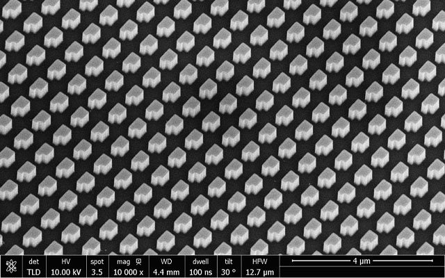
Arrays of dielectric or plasmonic resonators (metasurfaces or photonic crystals) or single nanoantennascan be fabricated using a variety of tools and techniques including electron beam lithography, liftoff, etching, focused ion beam milling, etc.
-
We routinely fabricate metasurfaces of dielectric materials such as TiO silicon and a variety of III-V semiconductors such as GaAs, InGaAs, AlGaAs, etc.
-
The metasurfaces can be patterned directly onto the semiconductor substrates or transferred onto transparent substrates such as quartz or sapphire.
-
Typical dimensions range from 50 to hundreds of nanometers or microns.
-
Target wavelengths can range from the visible to the mid–far infrared.
Contact: Igal Brener
Research Highlight:
Strong Coupling in the Sub-Wavelength Limit Using Metamaterial Nanocavities
Benz, A.; Campione, S.; Liu, S.; Montaño, I.; Klem, J. F.; Allerman, A.; Wendt, J. R.; Sinclair, M. B.; Capolino, F.; Brener, I. Nature Communications 2013, 4 (1). doi.org/10.1038/ncomms3882