Center for Integrated Nanotechnologies

Helping you understand, create, and characterize nanomaterials

High Resolution Scanning Electron Microscope, Focused Ion Beam, and Electron Beam Lithography

Two FEI field-emission source SEMs in the Integration Lab at CINT

The Nova NanoSEM 450 includes a Nabity electron beam lithography (EBL) patterning capability. 
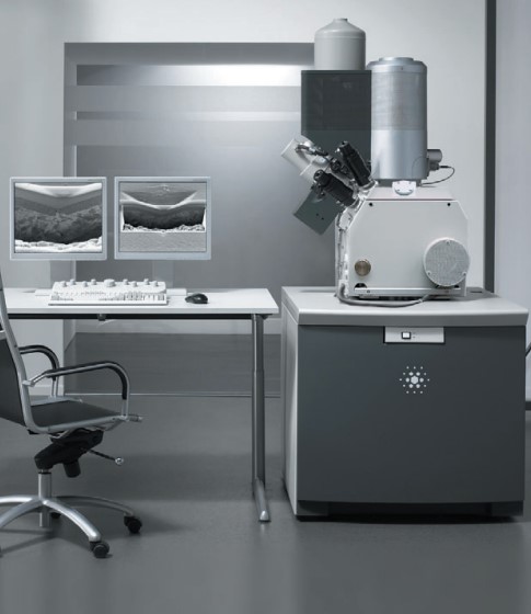
The Nova 600 Nanolab from FEI Company combines ultrahigh resolution SEM with FIB capabilities in one system for sample analysis, 2D and 3D machining, and prototyping. The resolution of 1.1 nm at 15 kV in secondary electron mode is further enhanced when using the STEM detector.  This dual-beam system also allows for electron and ion induced deposition of metals from gas source precursors (currently, Pt) with line widths of 50 nm (ion beam) and 20 nm (electron beam). An auto FIB, auto TEM, and pattern generation module is available for ion milling to provide automation of many
tasks. The system also includes a Nabity EBL patterning capability.

Contact: Doug Pete

Research Highlight:
Multicolor Three-Dimensional Tracking for Single-Molecule Fluorence Resonance Energy Transfer Measurements
Keller, A. M.; DeVore, M. S.; Stich, D. G.; Vu, D. M.; Causgrove, T.; Werner, J. H. Analytical Chemistry 2018, 90 (10), 6109–6115. doi.org/10.1021/acs.analchem.8b00244


Back to top