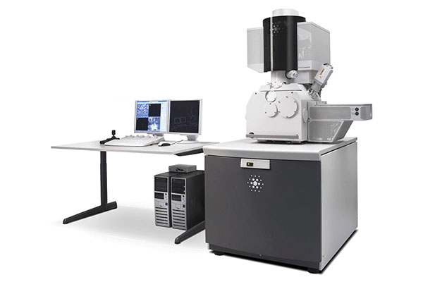
 The FEI Magellan 400 SEM provides sub-nanometer spatial resolution from 1kV to 30 kV. By using low voltages, only the surface of the sample interacts with the electron beam and thus insulators/beam sensitive samples can be imaged without the need for conductive coatings and the amount of surface data is maximized.
Technical Specifications:
- Our insertable STEM detector provides for quick imaging on TEM grids when atomic resolution isn’t needed and rapid turnaround is preferred.
- Schottky thermal emission source with UniColore mode to give a highly coherent beam (less than 0.2 eV energy spread).
- Spatial resolutions of 0.8 nm at 1kV and above in secondary electron mode.
- EDAX Octane Elect SDD Energy Dispersive Spectroscopy (EDS) detector for elemental analysis.
- EDAX Hikari Electron Backscatter Diffraction (EBSD) detector for crystallographic orientation determination.
- Nabity electron beam lithography patterning capability.
- Annular STEM detector (spatial resolution of 0.7 nm).
- Insertable CBS backscatter detector with amazing performance on charging samples.
- TMC passive and active vibration cancellation platform as well as full-system acoustic enclosure.
Research Highlight:
Mapping Emission from Clusters of CdSe/ZnS Nanoparticles
Ryan, D. P; Goodwin, P. M.; Sheehan, C. J.; Whitcomb, K. J.; Gelfand, M. P.; Van Orden, A. The Journal of Physical Chemistry C 2018 122 (7), 4046-4053. doi.org/10.1021/acs.jpcc.7b10924
 The FEI Magellan 400 SEM provides sub-nanometer spatial resolution from 1kV to 30 kV. By using low voltages, only the surface of the sample interacts with the electron beam and thus insulators/beam sensitive samples can be imaged without the need for conductive coatings and the amount of surface data is maximized.