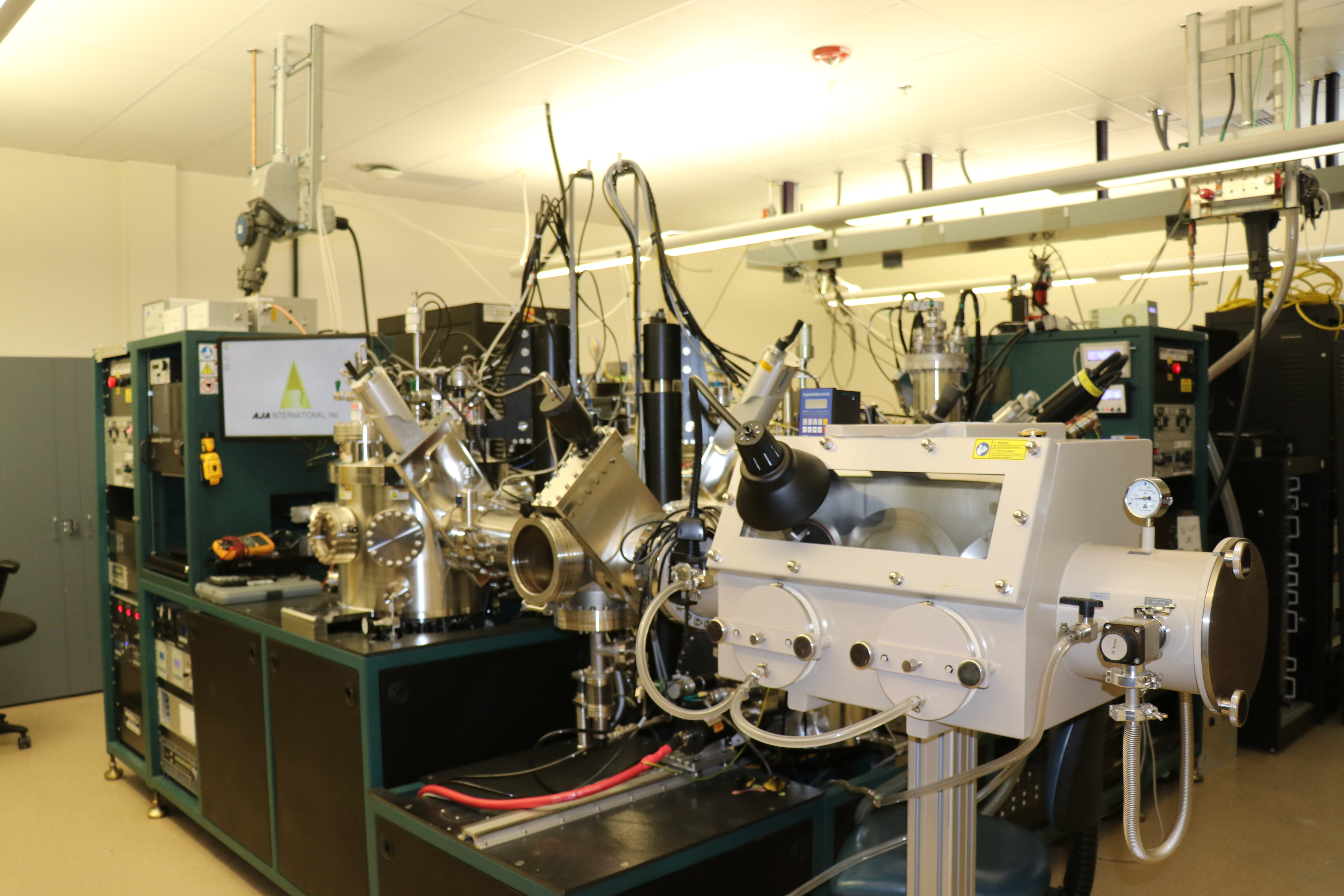
Advanced thin film synthesis using a suite of physical vapor deposition (PVD) techniques. With multiple specialized deposition systems and integrated in-situ diagnostics, we support the growth of complex material systems with precise control over composition, structure, and properties. Heated and biased substrates allow fine control over microstructure (texture, density, grain size, and chemistry), while real-time diagnostics such as laser curvature tool, surface acoustic wave (SAW), and reflection high-energy electron diffraction (RHEED) provide insight into film evolution during growth.
Capabilities include:
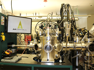
Magnetron sputtering (DC/RF/HiPIMS)
- 2" direct sputtering sources for co-deposition and multilayers
- 3" HiPIMS sources for metals and ceramics
- Pulsed DC power supply for reactive N2 or O2 sputtering
- RF power supplies for oxide deposition
- DC/RF substrate biasing
- 4" wafer handling
- 700 C sample heating
- Base pressure ~8.0 E-8 Torr
- In-Situ plasma monitoring, RGA, and strain measurement
- Glovebox for air-free sample handling
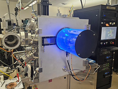
Dual Source E-Beam Evaporation
- Co-deposition and multilayer growth using dual e-beam sources
- Ion beam-assisted deposition capability
- Substrate biasing (DC/RF) and heating up to 700 °C
- 4" wafer handling
- Base pressure: ~4 × 10⁻⁸ Torr
- In-Situ RHEED for crystallographic monitoring
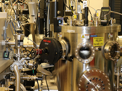
Dual Ion Beam Sputtering and Etching
- Ion beam-assisted deposition and etching
- Reactive ion beam sputtering (O₂, N₂, Ar
- Ideal for low process pressure deposition
- Substrate heating up to 800 °C
- 4" wafer handling
In-Situ Diagnostics
- RHEED — crystallography and growth mode
- Laser curvature — internal stress evolution
- Surface Acoustic Wave (SAW) — elastic properties and modulus
- Plasma monitoring & RGA — process chemistry and stability
Characterization
- X-Ray Photoelectron Spectroscopy (XPS) — surface chemistry (STAIB Instruments)
- Scanning Electron Microscopy (SEM) — morphology and microstructure (STAIB Instruments)
- Auger Electron Spectroscopy (AES) — elemental analysis (3–10 keV)
- X-Ray Fluorescence (XRF) — compositional mapping
- Profilometry (DekTak) — thickness, roughness, and stress measurements
Contact:
Hyosim Kim
Research Highlight:
Effects of Substrate Temperature and Deposition Rate on the Phase Separated Morphology of Co-Sputtered, Cu-Mo Thin Films
Derby, B.; Cui, Y.; Baldwin, J. K.; Misra, A. Thin Solid Films 2018, 647, 50–56. DOI:10.1016/j.tsf.2017.12.013.