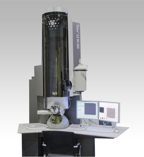
Aberration-corrected STEM with EDS and EELS allows us to both image and perform microanalysis of materials in the same experiment connecting structure and chemistry at nanometer and sub-nanometer length scales. Examples of materials analyzed include nanoparticles (e.g., core shell), epitaxial semiconductors and oxides, metals and alloys, battery materials, etc. We also have the ability to utilize most of the CINT specimen holders including cryogenic and heating.
Capabilities include:
Contact:
Paul Kotula
Ping Lu
Research Highlight:
Lu, P.; Zhou, L.; Kramer, M.J.; Smith, D.J. Scientific Reports. 2014, 4, 3945. doi.org/10.1038/srep03945
Analysis of Multilayer Devices for Superconducting Electronics by High-Resolution Scanning Transmission Electron Microscopy and Energy Dispersive Spectroscopy
Missert, N.; Kotula, P.G.; Rye, M.; Rehm, L.; Sluka, V.; Kent, A.D.; Yohannes, D.; Kirichenko, A.F.; Vernik, I.V.; Mukhanov, O.A.; Bolkhovsky, V.; Wynn, A.; Johnson, L.; Gouker, M. IEEE Trans.. Appl.. Supercond. 2017, 27, 1100704. doi.org/10.1109/TASC.2017.2669579